Google statistics

Showing posts with label PCB. Show all posts

Monday, 5 September 2016

Klon 3v3 Clone: Schematics and PCB layout

Klon 3v3 Clone Schematics

Klon 3v3 Clone schematics have been implemented using Eagle CAD. Op-amps used are TI LME49721, they are low-distortion, low-noise Rail-to-Rail Input/Output that can be powered between 2.2 and 5.5V. Passive values, resistors and capacitors have been changed to adapt to the power supply change from 9V to 3.3V, many of them have been multiplied by 3 and some of them adjusted to achieve a similar signal in all op-amp stages. Top gain potentiometer series resistor has been splitted into R4 and R5 on both sides of the potentiometer to avoid the low gain value obtained when this potentiometer is set to minimum. filter components around bottom gain potentiometer have been obtained by multiplying by 3 the original values.
Clipping diodes D1 and D2 are 1N34A germanium, they are not part of the BoM since they cannot be found through big distributors, specialized guitar pedal shops can stock them.
Gain resistors R7, R19, R23 have been tuned during simulations to obtain a similar saturation to original circuit on each stage, and then tweaked again on real circuit by ear. Note that values that appear in the BoM are those used on simulations and are lower than the final used values.
1nF capacitor C24 has been added for better circuit stability.

The 9V to 3.3V DC-DC converter is an integrated step-down controller TI TPS62122 in a tiny WSON-6 package. R29-R30 resistors set the FB reference voltage to get 3.3V on the output. A 22uH L1 inductor is required for the switching regulator. Switching frequency is as high as 800kHz, far from audible frequencies, but an additional LC filter, L2 100nH, C22 1uF has been added to reduce output ripple. recommended C19, C20 input output decoupling capacitors have been added to input and output respectively.

Mid 1.65V reference voltage for op-amps bias is generated by LM4041 reference voltage IC.

FB1-FB2 BLM31PG121SN1L are 120ohm ferrites to filter input and out signals respectively

9V input power supply is filtered using CF1 Murata NFM3DPC223R1H3L 22nF EMI filter.

D3 is an input power protection for inverted voltage.

The Klone 3v3 Clone BoM can be found on this link. Please review it before buying the components. Components used are SMD 0402 whenever possible.
Klon 3v3 Clone Eagle CAD Schematics

Klon 3v3 Clone PCB layout

Circuit has been implemented on a 54 x 54 mm 2-layer PCB that fits into a 1590B enclosure. 3.3V power supply is routed as a plan on top layer, and GND is routed as a plan on bottom layer.
Klone 3v3 Clone PCB layout: Top layer
Klone 3v3 Clone PCB layout: Bottom layer

Sunday, 15 May 2016

DMFX-1-2 (mezzanine board) PCB layout and assembly

DMFX1-2 is the DMFX-1 system mezzanine board.

DMFX1-2 requires a more standard, less demanding and cheaper PCB technology than DMFX1-is DMFX1-2 consists of 2-layers on FR4 dielectric (100 x 68mm). green soldermask, and white top silkscreen, layer plated copper thickness is 35μm. PCB thickness is 1.55mm. Minimum trace width is 250μm and minimu isolation distance is 250 μm. Minimum finished hole is 350μm.
It uses an Eurocircuits class 3B compared to class 8D for DMFX1-1.

The mezzanine board is plugged into the main board using 2 high density connectors, it houses a 128x32 pixel LCD graphic display blue LED with white LED backlight, a 5-button integrated switch with 4 arrow buttons (left, right, up, down) and a center OK button that allows navigating through menus displayed on LCD, five red LEDs, and 5 potentiometers connected to SAR ADC inputs on control DSP.

Top layer is used for signals and power plane. Bottom layer is used for signals and ground plane
DMFX1-2: Top layer
DMFX1-2: Bottom layer
This is the DMFX1-2 mezzanine board fully assembled:
DMFX1-2 fully assembled


DMFX-1-2 (mezzanine board) Schematics and BoM

DMFX-1-2 is a mezzanine board that get plugged into the main board DMFX1-1 by means of two 20-pins SMD connectors on the bottom side of the PCB.
The mezzanine board includes a  LCD-graphic 128x32 pixels display panel (with 
blue background white pixels and white backlight) that is configured from control DSP-2 via an SPI bus.
It also includes a button navigator with five switches (four arrow buttons: Up, down, left, right and center OK button) used to navigate through the LCD menus.

Additionally, there are five 3-mm red LEDs and five 9-mm potentiometers. A 5K potentiometer (VR5) in the middle, controls the distortion octaver level. The other four 50K potentiometers (VR1-4X) are connected to analog SAR ADC inputs (AIN0-3) on DSP-1. Only two of them (VR3-4) are connected to DSP-2 (AIN2-3) since AIN0-1 are connected to tuner and noise suppression circuits respectively.
These may be used as digital potentiometers to configure some effect parameters such as gain, volume, tone, depth, delay, rate... on LCD menu.
DMFX-1-2: Schematics

Schematics and BoM source files

Schematics and layout have been made using CAD Eagle 6.3.0. Source files can be found in the DMFX-1-2 github HW repository including Eagle Schematics source files (.sch), Eagle Board layout files (.brd), Eagle component libraries (.lbr), Schematics in pdf format, and all manufacturing files including gerber files, assembly drawings and pick and place files. An Excel file contains the full BoM including reference designators, manufacturer part number  as well as Digikey part number.

DMFX-1-1 (main board) PCB layout and assembly

DMFX-1 consists of two PCBs built by Eurocircuits:
  1. Main board (from now on DMFX-1-1) is 8-layers on FR4 dielectric (144 x 100mm), green soldermask and white top-bottom silkscreen, inner layer copper thickness is 18 μm (1/2 oz.), outer plated copper layer is 30 um. PCB thickness is 1.55 mm. Outer layers traces are 125μm, inner layer traces 100μm, isolation distances are 100μm. Hole density  <1000/dm2. Minimum finished hole is 150μm. This corresponds to Eurocircuits pattern class 8 drill class D.
  2. Mezzanine board (from now on DMFX-1-2) is 2-layers on FR4 dielectric (100 x 68mm). green soldermask, and white top silkscreen, layer plated copper thickness is 35μm. PCB thickness is 1.55mm. Minimum trace width is 250μm and minimu isolation distance is 250 μm. Minimum finished hole is 350μm. This corresponds to Eurocircuits pattern class 3, drill class B.

Here you can verify Eurocircuits pattern classification. DMFX-1-1 requires a quite high and therefore more expensive pattern and drill class (8D)
The main reason for that is that DSPs are 144-pin 0.8 mm pitch BGA devices. The main challenge of this project is using those tiny BGAs with 0.8 mm pitch which are not very well suited for a DIY application, and the biggest challenge of all is manually soldering those BGAs
But 0.8 mm pitch BGAs also impose constraints on minimum trace width and the number of layers to be able to fanout all the BGA pins.
If minimum finished plated drill (PTH) size is 150μm for class D, minimum production hole diameter (PHD) size is 250μm and minimum inner/outer annular ring (IAR/OAR) is 100μm, which corresponds to a via pad size of 450μm (PTH + 2xOAR/IAR = 250+100+100)
That means that between two 450μm vias spaced 800μm there is a distance of 350μm within which we have to pass fanout traces, class 7 requires 125μm traces an isolation and hence 3x125μm=375μm. Conclusion: a class 8D is required with minimum trace width 125μm and minimum isolation of 100μm.
DMFX-1-1: PCB design rules
There are four signal layers: top, bottom and internal layers 3 and 4, but all signal layers include ground planes (analog and digital), this helps copper balancing on PCB but also it helps to shield and reduce noise if some via stitching is added so that good ground connection is assured on all layers.
Layer 3 uses mainly horizontal routing and layer 4 uses vertical routing.
Layers 2 and 5 are mainly ground and power planes.

DMFX-1-1: Top layer - layer 1 (signals)
DMFX-1-1: Layer 3 (signals, horizontal routing)
DMFX-1-1: Layer 4 (signals, vertical routing)
DMFX-1-1: Layer 5 (Power planes)
DMFX-1-1: Bottom layer - layer 6 (signals)
DMFX-1-1: Assembly top

Notes:

It is recommended to move capacitor C180 down as indicated by the red arrow in the following figure, below the line marked by the green arrow that shows the position of the border of the mezzanine board. C180 electrolytic capacitor is too high and mezzanine board may not be fully plugged in.

DMFX-1-1 (main board) schematics and BoM

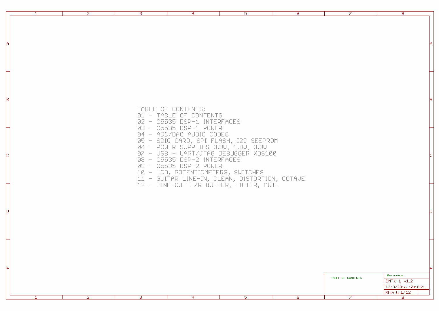
DMFX-1-1 includes the following blocks:
  • TI C5535 DSP-1 implements the digital effects and audio codec control (pages 2-3)
  • TI AIC3204 ADC/ADC audio codec and buffer, 12MHz clock oscillator, stereo headphones output jack (page 4)
  • DSP-1/2 external memories: SPI, I2C, SD/MMC (page 5)
  • DC/DC step-down switching regulators (3.3V, 1.8V) and LDO (1.3V), power-on reset, clock driver (page 6)
  • FTDI2232 USB/JTAG interface an SEEPROM (page 7)
  • TI C5535 DSP-2 implements LCD, navigator buttons, tuner control (page 8)
  • DMFX-1-2 mezzanine Connectors and footswitch push-button (page 9-10)
  • Line-In stereo input buffer, filters, distortion circuit (page 11)
  • Line-Out dual-mono output buffers and filters, tuner, noise supressor circuits (page 12)
DMFX-1-1: Schematics page 1 - Table of Contents
    DSP-1 implements the digital effects and control the audio codec. It includes a dedicated mini-USB connector. Four analog SAR ADC input are connected to DMFX-1-2 potentiometers. DSP-1 is the first device on the JTAG daisy chain connected to USB/JTAG device to allow JTAG emulation and debugging. INT0 input is connected to DSP-2 external flag (XF) signal and DSP-1 XF signal is connected to DSP-2 INT0; both DSPs exhange interrupts to allow synchronizing processes and tasks between both processors. INT1 is connected to DSP-1 GPIO10. Two SD/MMC cards are connected to DSP-1 to store data, samples, loops, code...
    I2S2 interface is a fast serial interface to exchange samples between DSP-1 and ADC/DAC on audio codec. SPI interface is connected to an external SPI flash to store code and data. UART interface is connected to CBUS on USB/JTAG-UART device and it can be used as console for emulator debugging. I2C bus is connected to external SEEPROM, to store parameters or inventory information. I2C is used for configuring audio codec, and it is also connected to DSP-2 to exchange FX configuration parameters set by user interface via LCD menu and buttons.
    DMFX-1-1: Schematics page 2 - DSP-1 FX interfaces
    Page 2 shows DSP-1 power supply inputs, ferrite filters and decoupling capacitors.
    DMFX-1-1: Schematics page 3 - DSP-FX power

    Page 3 shows TI TLV320AIC3024 audio codec that includes ADC/DAC, LINE input, MIC input, LINE out and stereo headphones amplifier. I2S is a high speed serial interfaces to echange audio samples with DSP-1 at a sampling frequency configured by DSP-1. Interface is buffered via a CBTLV3245 octal bus switch. 12MHz clock oscillator is included here, it is connected to a clock driver on page 6.
    DMFX-1-1: Schematics page 4 - Audio CODEC ADC/DAC
    Page 5 includes two W25Q64 64-Mbit SPI flashes connected to each DSP SPI interface. Two SD/MMC cards are connected to DSP-1 for large storage (samples, loop, data). One I2C 64Kbit SEEPROM 24C64 can be used to store remote inventory or configuration data.
    DMFX-1-1: Schematics page 5 - Memories I2C, SPI, MMC
    Page 6 shows two DC/DC step-down switching regulators TI TPS56220. They generate +3.3V and +1.8V respectively from a +9V external supply or +5V USB input with a maximum current of 500mA each. A TI TPS73201 LDO generates the analog 1.3V DSP supply voltage from 1.8V input at a maximum current of 250 mA. A TI CDCLVC1108 octal clock buffer generates up to 8 clocks from 12MHz clock oscillator: USB DSP-1 clock, DSP-1 system clock, audio codec master clock, USB/JTAG clock, USB DSP-2 clock and DSP-2 system clock.
    DMFX-1-1: Schematics page 6 - power supply, clock driver
    Page 7 shows an FTDI2232 USB/JTAG interface device that works as XDS100v2 TI emulator for DSP debugging. ABUS is connected to JTAG daisy chain on DSP-1 and DSP-2. CBUS is sonnected to UART interface on DSP-1. A D-type flip-flop detects power reset rising edge from FTDI device and generates a power detect signal back to the FTDI device. An external SPI SEEPROM AT93C46 stores USB device configuration parameters. USB port is protected for ESD. USB debug port is a type-B USB connector. The +5V USB debug port can be used to power the whole DMFX-1 system. DMFX-1 system can actually be powered from any of the three USB ports or by an external +9V power supply.
    DMFX-1-1: Schematics page 7 - USB/JTAG
    DSP-2 implements user interface and control tasks. It includes a dedicated mini-USB connector. Two analog SAR ADC inputs (AIN0-1) are connected to tuner circuit output and noise supression circuit output respectively, AIN2-3 are connected to DMFX-1-2 potentiometers 2-3. DSP-2 is the second device on the JTAG daisy chain connected to USB/JTAG device to allow JTAG emulation and debugging. INT0 input is connected to DSP-1 external flag (XF) signal and DSP-2 XF signal is connected to DSP-1 INT0; both DSPs exchange interrupts to allow synchronizing processes and tasks between both processors. INT1 is connected to DSP-2 GPIO10.
    DSP-2 GPIO0 controls clean or distorion audio input to audio codec. GPIO1-2 configure the overdrive/distortion gain, GPIO3-4 control different overdrive/distortion modes, increasing mid tones or setting fuzz clipping diodes circuit. GPIO6-11 drive five red LEDs on DMFX-1-2 mezzanine board. GPIO11 is connected to CPU active green LED.
    SPI interface is connected to SPI flash (device 0) and to 128x32 graphic LCD (device 1) on DMFX-1-2 mezzanine board, GPIO12 is connected to LCD A0 signal and is used to send command or data to LCD via SPI bus. GPIO13-17 are connected to the five navigator buttons respectively: left, up, center, down, right.
    GPIO28 is connected to footswitch.
    SPI and UART interfaces are not used. I2C bus is connected to DSP-1 to exchange FX configuration parameters set by user interface via LCD menu and buttons.
    DMFX-1-1: Schematics page 8 - DSP-2 Control interfaces
    Page 9 shows DSP-2 power supply inputs, ferrite filters and decoupling capacitors.
    DMFX-1-1: Schematics page 9 - DSP-2 Control Power
    Page 10 shows DMFX-1-2 mezzanine connectors. J5 connector includes DSP-2 SPI2 bus, LCD A0 addess signal, reset signal and the five navigator button inputs: left, up, center, down, right. J7 connector includes LED1-5, DSP-1 GPAIN0-3 SAR ADC signals, DSP-2 GPAIN2-3 SAR ADC signals, distortion circuit output, octave circuit output and the mix of distortion-octave coming from a potentiometer on DMFX-1-2. +3.3V, analog +1.3V power supplies and ground.
    DMFX-1-1: Schematics page 10 - Connectors
    Input buffers and filters and distortion circuits are based on TI rail-to-rail LME49721 audio op-amps powered at +3.3V, in contrast with +9V supply normally used on guitar pedals. 

    Overdrive/Distortion:

    First opamp stage has 0dB gain but implements some low pass filtering. Second op-amp stage implements a configurable gain controlled by DSP-2 GPIO signals connected to OD_DRV0-1. when both switches are active (shorted) we obtain the minium gain value of 13dB (x4.5), if OD-DRV1 is open, gain value is incremented by 10dB (x14.5), if OD_DRV0 is open, gain value is incremented by 9dB (x40). Third op-amp stage implements high saturating gain (hard clipping) or soft clipping via asymmetric diodes, when OD_MODE1 is 0, a 20dB gain is implemented with 10K switch shorted and switch in series with diodes open. When OD_MODE0 is 1, a 10dB gain is implemented, but soft asymmetric clipping is added with Schottky diodes added in parallel to the opamp feedback path.

    OD_MOD0 activates a notch filter that attenuates middle tones by 12dB at 400Hz.

    These four GPIOs: OD_DRV0-1 and OD_MODE0-1 allow different combinations of gain, hard clipping, soft clipping, and mids attenuation to get different types of analog overdrive and distortion effects.

    Octave-up:

    A forth op-amp implements a full-wave rectification that generates a octave up, that can be mixed with distortion output.

    Line-In circuit:

    The input from a guitar can be connected to Line-In input. The first stage is a J-FET buffer, followed by a filter that boosts up to 6dB high frequencies and attenuates down to 9dB low frequencies. 0dB occurs at 3.7kHz. The filtered line-in signal is the input to the tuner circuit and to an analog switch that can select the clean or the distortion at its output. The output of the switch is connected to the Audio Codec analog left channel input. Right channel input is connected to the clean signal, this allows mixing clean and distorted signal within DSP and obtain a more or less overdriven signal.
    The op-amp at the bottom of the page is a follower buffer that generates a middle point reference signal at 1.65V equal to 3.3V/2. Op-amps are rail-to-rail TI LME49721 powered at 3.3V.
    DMFX-1-1: Schematics page 11 - Input buffers, filters, clean, distortion
    Page 12 shows right and left channel pre-amp circuit with high impedance Line-Out signals that can be connected to a guitar amplifier or Line-In input of a sound card or sound equipment.This pre-amp amplifies 9dB with a 3dB bandwidth of 1.35kHz, 0dB is at 4kHz. The first op-amp stage filter is a low pass filter with a pole at approximately 14kHz and 3dB bandwisth at 24 kHz.

    The two op-amp circuit at the bottom of the page is used as support to the tuning and noise suppression circuit within the control DSP-2. The first stage is a very high gain amplifier that can be used as power detector for a noise suppression algorithm. The second op-amp is used as comparator and generates a square wave between 0 and full scale with the same fundamental frequency as the input signal and zero voltage when no signal is present. This square wave simplifies tuning algorithm using and auto-correlation method. Both tuner and noise suppression signals are connected to analog inputs of SAR ADC circuits within the Control DSP-2
    DMFX-1-1: Schematics page 12 - Output buffers, filters, tuner, noise suppression

    Schematics and BoM source files

    Schematics and layout have been made using CAD Eagle 6.3.0. Source files can be found in the DMFX-1-1 github HW repository including Eagle Schematics source files (.sch), Eagle Board layout files (.brd), Eagle component libraries (.lbr), Schematics in pdf format, and all manufacturing files including gerber files, assembly drawings and pick and place files. An Excel file contains the full BoM including reference designators, manufacturer part number  as well as Digikey part number.

    For your convenience here is a link to DigiKey with a BoM of the whole DMFX-1 platform including main board DMFX-1-1, described in this post, and the daughter board (DMFX-1-2 with LCD and navigator buttons). You'd better verify BoM completion, lead-times and obsolescent components beforehand.

    With all this information you can build your own DMFX-1 platform and develop your own Digital effects!!

    Monday, 8 September 2014

    Tube Simulator - Practical Implementation - PCB layout, manufacturing, assembly (2/4)

    PCB layout


    The PCB has been designed in two layers, using a maximum of ground and power planes surface and numerous vias, specially in the central ground pads below ICs that dissipate more power: regulators and power audio amplifiers.

    PCB width is mostly imposed by the front panel controls: switches, potentiometers and jacks.
    With that in mind a proper aluminum box was chosen:
    Hammond Manufacturing 1444-1372 13 x 7 x 2 inches (W x D x H) 

    The L shape of the PCB leaves some space for AC power inlet, AC power switch, 1A AC fuse, AC/DC power supply, and the posibility of adding a PCB module for FX loop effects or digital reverb circuit (these modules have not been implemented yet)

    Top layer


    Bottom layer


    PCB manufacturing


    For PCB manufacturing I used Eurocircuits web site. Eagle CAD files can be uploaded and there is a very practical Price Calculator that allows having immediate quotes with options for standard pool or PCB prototypes for small PCBs . They also have the possibility to verify the PCB layout after file uploading.
    I paid 140 euros (transport and taxes included) for one prototype on a 7 day working days delivery. Usually is recommended to manufacture at least two prototypes. PCBs are manufactured in Europe, they have a factory in Hungary.

    Quality is very good with nice finish:

    PCB assembly


    The assembly drawing and the PCB ready for soldering components. SMD DC-DC converters with central pads where previously mounted using solder paste and hot soldering gun.
    The solder paste that appears in the photo below was purchased in a generic DIY store and created lots of problems of oxidation. I recommend using a solder paste specific for electronic use with lowt melting temperature, usually RoHS (not leaded) solder pastes have a quite high melting point, but there are some RoHS compatible solder pastes like alloy 58 Bi / 42 Sn with a melting point as low as 138°C. The one I use is EDSYN - CR11 58/42 Bi/Sn from Farnell

    It is very important to leave thermal reliefs on pads, specially in a design like this with large power and ground planes, otherwise solder iron heat will dissipate through the plane and soldering those pads will be a nightmare. I know because it happened to me.

    The PCB with most of the components soldered. Rear connectors must be soldered with wires to allow PCB assembly in the chassis.

    The AC/DC power supply module used was a Murata MVAD040-24 40W (23 euros) open switching power supply module with 120/230V AC@50/60Hz input and +24V DC@1.67A 40W. 


    PCB mounted on the chassis aluminium base plate, with AC/DC power supply, 1A AC fuse and AC power switch: