Google statistics

Showing posts with label BoM. Show all posts

Tuesday, 1 May 2018

NuTube Overdrive - Schematics, BoM, PCB layout, 3D

Disclaimer

This is just an amateur pedal with no intention for profit or to infringe any trademark.
Tube Screamer is a trademark of Hoshino Gakki Co.
Nutube is a trademark of KORG INC.
This pedal is not for sale. If you want to buy a similar pedal I recommend you Ibanez NTS Screamer.

Schematics

Some ferrites are used to filter noise at the input and output. +9VDC power voltage is also filtered by means of an EMI filter Murata NFM3DPC223R.
Op-Amps +4.5V mid voltage is generated by a LM4041 voltage reference.
Grid DC bias voltage is generated from +5V DC-DC output via a 4K7 resistor in series with a 10K trimmer. The trimmer midpoint is filtered with 10µF capacitor and connected to the grid via 33K resistor as recommended by manufacturer.
An MMBT5089 NPN transistor buffer is used between the two triode sections.
NPN buffers are also connected at the input and the output of the pedal.
An Op-Amp buffer is used at the output of the second triode section, the buffer output is connected to the 100K Mix linear potentiometer.
NuTube triodes have 500K linear trimmers on anode loads connected to +9VDC.
+5VDC is connected via 240R series resistor and filtered with 1µF capacitors to provide the required filament voltage to triodes.
R8 and R38 pull-down resistors are required to avoid popping when engaging or disengaging the effect via true-bypass 3PDT footswitch.
S1 is the switch that allows disconnecting the clipping diodes. BAV199 are dual diodes in a single SOT23 package. R14 shorts one of the diodes to provide asymmetrical clipping.
R13 can be removed to disconnect C8 220nF capacitor and disable bass-boost mod.
The output of the mix potentiometer is connected to the tone section via an Op-Amp buffer.
Volume potentiometer is a 100K audio/log taper.

NuTube Screamer Schematics, page 1
NuTube triodes require a +5VDC filament voltage with 200mA current per triode . A TPS62175DQCR DC-DC converter generates +5VDC 500mA from +9VDC input. +5V is also used to generate grid DC bias between +2V and +3V.

NuTube Screamer Schematics, page 2. Grid bias voltage +5V DC-DC converter

Bill of Materials


Part Number Mfg Name Description Qty Reference Value
CRCW06030000ZSTB Vishay Thick Film Resistors - SMD 0603 1/10watt ZEROohm Jumper 2 R13, R14 0R
ERJ-3EKF1001V Panasonic Thick Film Resistors - SMD 0603 1Kohms 1% Tol 7 R5, R9, R16, R23, R25, R27, R33 1K
CR0603-FX-1004ELF Bourns Thick Film Resistors - SMD 0603 1M 1% 1/10W 7 R3, R7, R8, R11, R24, R26, R31 1M
C1608X7R1V105K080AE TDK CAP CER 1UF 35V 10% X7R 0603 8 C3, C4, C5, C6, C7, C18, C19, C23 1u
RC0603FR-073K3L Yageo Thick Film Resistors - SMD 0603 3.3kohms 1% Tol 1 R28 3.3k
ERJ-3EKF4701V Panasonic Thick Film Resistors - SMD 0603 4.7Kohms 1% Tol 1 R15 4.7k
C2012X5R1E475K125AB TDK CAP CER 4.7uF 25volts X5R 10% 0805 2 C21, C31 4.7u
ERJ-3EKF4701V Panasonic Thick Film Resistors - SMD 0603 4.7Kohms 1% Tol 1 R35 4k7
CR0603-FX-1002HLF Bourns Thick Film Resistors - SMD 0603 10KOHM 1/10WATT 1% 6 R1, R2, R10, R12, R22, R32 10k
GRM21BR6YA106KE43L Murata CAP CER 10UF 35V X5R 0805 15 C1, C2, C10, C12, C13, C14, C15, C16, C17, C20, C24, C25, C26, C30, C33 10u
SRN4018-100M Bourns FIXED IND 10UH 1.3A 180 MOHM SMD 1 L1 10u
C2012X5R1V226M125AC TDK CAP CER 22UF 35V X5R 0805 1 C32 22u
CR0603-FX-3302ELF Bourns Thick Film Resistors - SMD 0603 33K ohm 1% 2 R17, R18 33k
06035D473MAT2A AVX CAP CER 0.047UF 50V X5R 0603 2 C9, C29 47n
GCM1885C2A470JA16D Murata CAP CER 47PF 100V C0G/NP0 0603 1 C11 47p
ERJ-3EKF5102V Panasonic Thick Film Resistors - SMD 0603 51Kohms 1% Tol 1 R19 51k
RC0603FR-0768KL Yageo Thick Film Resistors - SMD 0603 68kohms 1% Tol 1 R34 68k
ERJ-3EKF8202V Panasonic RES SMD 82K OHM 1% 1/10W 0603 1 R41 82k
RC0603FR-07100RL Yageo RES SMD 100 OHM 1% 1/10W 0603 1 R29 100
ERJ-3EKF1003V Panasonic RES SMD 100K OHM 1% 1/10W 0603 2 R6, R40 100k
EEE-1VA101XP Panasonic CAP ALUM 100UF 20% 35V SMD 1 C22 100u
RC0603FR-07180KL Yageo Thick Film Resistors - SMD 0603 180K 1% 1/10W 1 R36 180k
ERJ-PA3F2200V Panasonic RES SMD 220 OHM 1% 1/4W 0603 2 R30, R37 220
GRM188R61H224KAC4D Murata CAP CER 0.22UF 50V X5R 0603 3 C8, C27, C28 220n
ERJ-3EKF2400V Panasonic RES SMD 240 OHM 1% 1/10W 0603 2 R20, R21 240
CR0603-FX-4303ELF Bourns Thick Film Resistors - SMD 0603 430K ohm 1% 1 R39 430k
CR0603-FX-5103ELF Bourns Thick Film Resistors - SMD 0603 510kohms 1% Tol 1 R4 510k
PTV09A-4020S-A104 Bourns Potentiometers 9mm 100Kohms Audio 1 VOL A100K
PTV09A-4020F-B502 Bourns Potentiometers 9mm 5Kohms Linear 1 TONE B5K
3314G-2-103E Bourns TRIMMER 10K OHM 0.25W SMD 1 RV1 B10k
PTV09A-4020S-B104 Bourns Potentiometers 9mm 100Kohms Linear 1 MIX B100K
PTV09A-4020S-B504 Bourns Potentiometers 9mm 500Kohms Linear 1 GAIN B500K
3314G-1-504E Bourns TRIMMER 500K OHM 0.25W SMD 2 VR1, VR2 B500k
BAV199235 NXP Rectifiers DIODE LOW LEAKAGE 2 D1, D2 BAV199
BLM31PG121SN1L Murata EMI Filter Beads Chips & Arrays 1206 120 OHM 2 FB1, FB2 BLM31PG121SN1L
PJ-202A CUI CONN POWER JACK 2.1MM PCB 1 J2 DCJ0202
SSL-LX5093GD Lumex LED GRN DIFF 5MM ROUND T/H 1 LED1 GREEN
NMJ4HCD2 REAN Phone Connectors 2C MONO 2-SPST NC 1 J1 INPUT
LM4041CIDBZR Texas Instruments Voltage References Adjustable Precision Mcrpwr Shunt .5% 1 U4 LM4041CIDBZ
LME49723MA/NOPB Texas Instruments Audio Amplifiers Dual Audio Op Amp 2 U1, U3 LME49723
MBR0520LT1G ON Semiconductor Schottky Diodes & Rectifiers 0.5A 20V 1 D3 MBR0520LT1G
MMBT5089 Fairchild Semiconductor Transistors Bipolar - BJT NPN Transistor General Purpose  3 T1, T2, T3 MMBT5089
NFM3DPC223R1H3L Murata EMI/RFI Suppressors & Ferrites 0.022uF 50V 2A' 1 CF1 NFM3DC
831-87-032-10-001101 APEM Inc. Conn SIP Socket Strip SKT 32 POS 2mm Solder ST Thru-Hole 1 U2 NUTUBE 6P1
NMJ4HCD2 REAN Phone Connectors 2C MONO 2-SPST NC 1 J3 OUTPUT
TPS62175DQCR Texas Instruments IC REG BUCK BST ADJ 0.5A 10WSON 1 U5 TPS62175DQCR
MHS122K APEM Inc. SWITCH SLIDE SPDT 300MA 30V 1 S1 clip

PCB Layout

Top side

This is where all SMD components are mounted

NuTube Screamer PCB layout Top side (components)

Bottom side

This is where all the connectors and through-hole components are mounted: DC jack, input/output jacks, switch, potentiometers, LED and battery clipping contact for GND contact with enclosure
NuTube Screamer PCB layout Bottom side (connectors)
The following figure shows NuTube Screamer PCB pedal dimensions 72 x 54 mm and 1590B enclosure internal dimensions 107 x 55.45 mm
NuTube Screamer PCB and 1590B enclosure dimensions

3D assembly

Eagle layout can be imported into FreeCAD 3D to create a 3D assembly image that allows placing the different holes in the assembly and checking proper mechanical assembly.
LED had to actually be moved because it interfered with tone pot.

NuTube Screamer 3D assembly drawing

Sunday, 15 May 2016

DMFX-1-1 (main board) schematics and BoM

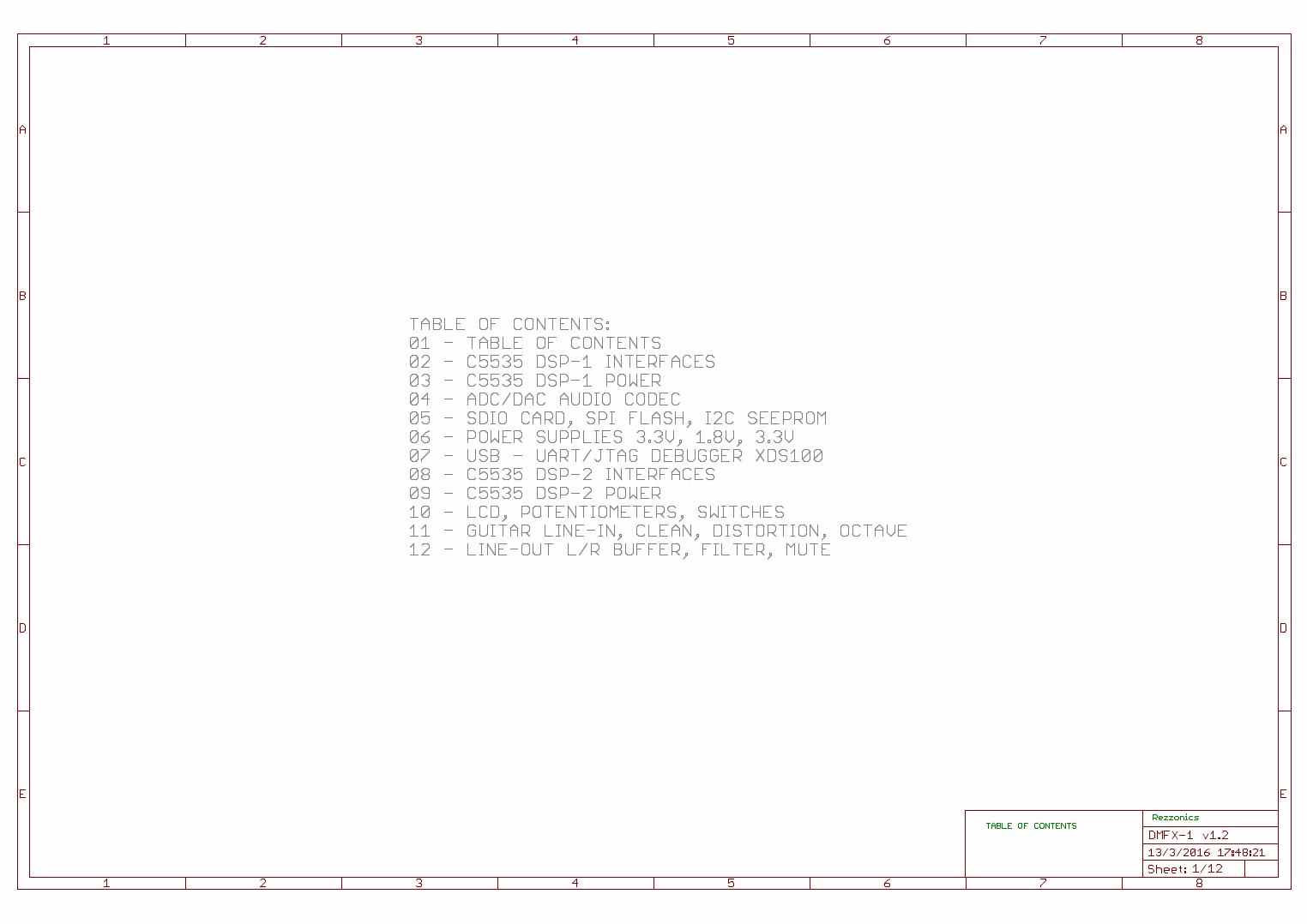
DMFX-1-1 includes the following blocks:
  • TI C5535 DSP-1 implements the digital effects and audio codec control (pages 2-3)
  • TI AIC3204 ADC/ADC audio codec and buffer, 12MHz clock oscillator, stereo headphones output jack (page 4)
  • DSP-1/2 external memories: SPI, I2C, SD/MMC (page 5)
  • DC/DC step-down switching regulators (3.3V, 1.8V) and LDO (1.3V), power-on reset, clock driver (page 6)
  • FTDI2232 USB/JTAG interface an SEEPROM (page 7)
  • TI C5535 DSP-2 implements LCD, navigator buttons, tuner control (page 8)
  • DMFX-1-2 mezzanine Connectors and footswitch push-button (page 9-10)
  • Line-In stereo input buffer, filters, distortion circuit (page 11)
  • Line-Out dual-mono output buffers and filters, tuner, noise supressor circuits (page 12)
DMFX-1-1: Schematics page 1 - Table of Contents
    DSP-1 implements the digital effects and control the audio codec. It includes a dedicated mini-USB connector. Four analog SAR ADC input are connected to DMFX-1-2 potentiometers. DSP-1 is the first device on the JTAG daisy chain connected to USB/JTAG device to allow JTAG emulation and debugging. INT0 input is connected to DSP-2 external flag (XF) signal and DSP-1 XF signal is connected to DSP-2 INT0; both DSPs exhange interrupts to allow synchronizing processes and tasks between both processors. INT1 is connected to DSP-1 GPIO10. Two SD/MMC cards are connected to DSP-1 to store data, samples, loops, code...
    I2S2 interface is a fast serial interface to exchange samples between DSP-1 and ADC/DAC on audio codec. SPI interface is connected to an external SPI flash to store code and data. UART interface is connected to CBUS on USB/JTAG-UART device and it can be used as console for emulator debugging. I2C bus is connected to external SEEPROM, to store parameters or inventory information. I2C is used for configuring audio codec, and it is also connected to DSP-2 to exchange FX configuration parameters set by user interface via LCD menu and buttons.
    DMFX-1-1: Schematics page 2 - DSP-1 FX interfaces
    Page 2 shows DSP-1 power supply inputs, ferrite filters and decoupling capacitors.
    DMFX-1-1: Schematics page 3 - DSP-FX power

    Page 3 shows TI TLV320AIC3024 audio codec that includes ADC/DAC, LINE input, MIC input, LINE out and stereo headphones amplifier. I2S is a high speed serial interfaces to echange audio samples with DSP-1 at a sampling frequency configured by DSP-1. Interface is buffered via a CBTLV3245 octal bus switch. 12MHz clock oscillator is included here, it is connected to a clock driver on page 6.
    DMFX-1-1: Schematics page 4 - Audio CODEC ADC/DAC
    Page 5 includes two W25Q64 64-Mbit SPI flashes connected to each DSP SPI interface. Two SD/MMC cards are connected to DSP-1 for large storage (samples, loop, data). One I2C 64Kbit SEEPROM 24C64 can be used to store remote inventory or configuration data.
    DMFX-1-1: Schematics page 5 - Memories I2C, SPI, MMC
    Page 6 shows two DC/DC step-down switching regulators TI TPS56220. They generate +3.3V and +1.8V respectively from a +9V external supply or +5V USB input with a maximum current of 500mA each. A TI TPS73201 LDO generates the analog 1.3V DSP supply voltage from 1.8V input at a maximum current of 250 mA. A TI CDCLVC1108 octal clock buffer generates up to 8 clocks from 12MHz clock oscillator: USB DSP-1 clock, DSP-1 system clock, audio codec master clock, USB/JTAG clock, USB DSP-2 clock and DSP-2 system clock.
    DMFX-1-1: Schematics page 6 - power supply, clock driver
    Page 7 shows an FTDI2232 USB/JTAG interface device that works as XDS100v2 TI emulator for DSP debugging. ABUS is connected to JTAG daisy chain on DSP-1 and DSP-2. CBUS is sonnected to UART interface on DSP-1. A D-type flip-flop detects power reset rising edge from FTDI device and generates a power detect signal back to the FTDI device. An external SPI SEEPROM AT93C46 stores USB device configuration parameters. USB port is protected for ESD. USB debug port is a type-B USB connector. The +5V USB debug port can be used to power the whole DMFX-1 system. DMFX-1 system can actually be powered from any of the three USB ports or by an external +9V power supply.
    DMFX-1-1: Schematics page 7 - USB/JTAG
    DSP-2 implements user interface and control tasks. It includes a dedicated mini-USB connector. Two analog SAR ADC inputs (AIN0-1) are connected to tuner circuit output and noise supression circuit output respectively, AIN2-3 are connected to DMFX-1-2 potentiometers 2-3. DSP-2 is the second device on the JTAG daisy chain connected to USB/JTAG device to allow JTAG emulation and debugging. INT0 input is connected to DSP-1 external flag (XF) signal and DSP-2 XF signal is connected to DSP-1 INT0; both DSPs exchange interrupts to allow synchronizing processes and tasks between both processors. INT1 is connected to DSP-2 GPIO10.
    DSP-2 GPIO0 controls clean or distorion audio input to audio codec. GPIO1-2 configure the overdrive/distortion gain, GPIO3-4 control different overdrive/distortion modes, increasing mid tones or setting fuzz clipping diodes circuit. GPIO6-11 drive five red LEDs on DMFX-1-2 mezzanine board. GPIO11 is connected to CPU active green LED.
    SPI interface is connected to SPI flash (device 0) and to 128x32 graphic LCD (device 1) on DMFX-1-2 mezzanine board, GPIO12 is connected to LCD A0 signal and is used to send command or data to LCD via SPI bus. GPIO13-17 are connected to the five navigator buttons respectively: left, up, center, down, right.
    GPIO28 is connected to footswitch.
    SPI and UART interfaces are not used. I2C bus is connected to DSP-1 to exchange FX configuration parameters set by user interface via LCD menu and buttons.
    DMFX-1-1: Schematics page 8 - DSP-2 Control interfaces
    Page 9 shows DSP-2 power supply inputs, ferrite filters and decoupling capacitors.
    DMFX-1-1: Schematics page 9 - DSP-2 Control Power
    Page 10 shows DMFX-1-2 mezzanine connectors. J5 connector includes DSP-2 SPI2 bus, LCD A0 addess signal, reset signal and the five navigator button inputs: left, up, center, down, right. J7 connector includes LED1-5, DSP-1 GPAIN0-3 SAR ADC signals, DSP-2 GPAIN2-3 SAR ADC signals, distortion circuit output, octave circuit output and the mix of distortion-octave coming from a potentiometer on DMFX-1-2. +3.3V, analog +1.3V power supplies and ground.
    DMFX-1-1: Schematics page 10 - Connectors
    Input buffers and filters and distortion circuits are based on TI rail-to-rail LME49721 audio op-amps powered at +3.3V, in contrast with +9V supply normally used on guitar pedals. 

    Overdrive/Distortion:

    First opamp stage has 0dB gain but implements some low pass filtering. Second op-amp stage implements a configurable gain controlled by DSP-2 GPIO signals connected to OD_DRV0-1. when both switches are active (shorted) we obtain the minium gain value of 13dB (x4.5), if OD-DRV1 is open, gain value is incremented by 10dB (x14.5), if OD_DRV0 is open, gain value is incremented by 9dB (x40). Third op-amp stage implements high saturating gain (hard clipping) or soft clipping via asymmetric diodes, when OD_MODE1 is 0, a 20dB gain is implemented with 10K switch shorted and switch in series with diodes open. When OD_MODE0 is 1, a 10dB gain is implemented, but soft asymmetric clipping is added with Schottky diodes added in parallel to the opamp feedback path.

    OD_MOD0 activates a notch filter that attenuates middle tones by 12dB at 400Hz.

    These four GPIOs: OD_DRV0-1 and OD_MODE0-1 allow different combinations of gain, hard clipping, soft clipping, and mids attenuation to get different types of analog overdrive and distortion effects.

    Octave-up:

    A forth op-amp implements a full-wave rectification that generates a octave up, that can be mixed with distortion output.

    Line-In circuit:

    The input from a guitar can be connected to Line-In input. The first stage is a J-FET buffer, followed by a filter that boosts up to 6dB high frequencies and attenuates down to 9dB low frequencies. 0dB occurs at 3.7kHz. The filtered line-in signal is the input to the tuner circuit and to an analog switch that can select the clean or the distortion at its output. The output of the switch is connected to the Audio Codec analog left channel input. Right channel input is connected to the clean signal, this allows mixing clean and distorted signal within DSP and obtain a more or less overdriven signal.
    The op-amp at the bottom of the page is a follower buffer that generates a middle point reference signal at 1.65V equal to 3.3V/2. Op-amps are rail-to-rail TI LME49721 powered at 3.3V.
    DMFX-1-1: Schematics page 11 - Input buffers, filters, clean, distortion
    Page 12 shows right and left channel pre-amp circuit with high impedance Line-Out signals that can be connected to a guitar amplifier or Line-In input of a sound card or sound equipment.This pre-amp amplifies 9dB with a 3dB bandwidth of 1.35kHz, 0dB is at 4kHz. The first op-amp stage filter is a low pass filter with a pole at approximately 14kHz and 3dB bandwisth at 24 kHz.

    The two op-amp circuit at the bottom of the page is used as support to the tuning and noise suppression circuit within the control DSP-2. The first stage is a very high gain amplifier that can be used as power detector for a noise suppression algorithm. The second op-amp is used as comparator and generates a square wave between 0 and full scale with the same fundamental frequency as the input signal and zero voltage when no signal is present. This square wave simplifies tuning algorithm using and auto-correlation method. Both tuner and noise suppression signals are connected to analog inputs of SAR ADC circuits within the Control DSP-2
    DMFX-1-1: Schematics page 12 - Output buffers, filters, tuner, noise suppression

    Schematics and BoM source files

    Schematics and layout have been made using CAD Eagle 6.3.0. Source files can be found in the DMFX-1-1 github HW repository including Eagle Schematics source files (.sch), Eagle Board layout files (.brd), Eagle component libraries (.lbr), Schematics in pdf format, and all manufacturing files including gerber files, assembly drawings and pick and place files. An Excel file contains the full BoM including reference designators, manufacturer part number  as well as Digikey part number.

    For your convenience here is a link to DigiKey with a BoM of the whole DMFX-1 platform including main board DMFX-1-1, described in this post, and the daughter board (DMFX-1-2 with LCD and navigator buttons). You'd better verify BoM completion, lead-times and obsolescent components beforehand.

    With all this information you can build your own DMFX-1 platform and develop your own Digital effects!!