The following figure shows the Schematics used to compare the frequency response of NuTube 6P1 vs 12AX7 in starved mode:
12AX7 has a 1M pulldown on grid input while NuTube 6P1 has a bias circuit to adjust the bias voltage on the grid between 0V and 3.3V, connected to the grid via 33K series resistor, the typical grid current of 6uA has been added, since the model does not include this bias current.
Anode/plate output resistor load is 500K in both circuits.
Both circuits have anode/plate connected to +24V via a series resistor and a potentiometer to adjust load.
NuTube 6P1 has resistor values multiplied by 10 to be able to sweep around the maximum gain point.
The following figure shows the starved 12AX7 frequency response between 10 Hz and 20 kHz with anode load potentiometer varying from 0 to 1. A maximum gain of 24.6 dB is obtained with a load resistance of 50K
The following figure shows the NuTube 6P1 frequency response between 10 Hz and 20 kHz with anode load potentiometer varying from 0 to 1. A maximum gain of 15.9 dB is obtained with a load resistance of 400K.
NuTube 6P1 application note shows a gain of 14dB with anode powered at +12V and 17 dB with anode powered at +30V, which actually corresponds to simulations.
Bypass capacitors are also compared between 10nF and 10uF. NuTube 6P1 bypass capacitor value must be multiplied by 15 in order to have a similar response at lower frequencies:
Google statistics
Showing posts with label valve. Show all posts
Friday, 26 May 2017
Thursday, 25 May 2017
Korg NuTube 6P1 vs 12AX7 starved tube / valve: SPICE models
I purchased some KORG NuTube 6P1 triodes samples and I wanted to build a guitar preamp circuit to get the characteristic tube sound and distortion.
I could not find any guitar preamp amplifier schematics that would suit me so I decided to make my own circuit based on the reference circuit and add some gain, tone stack and volume controls
I am more of a "SPICE simulation" kind of guy than a "bread-boarding" guy, also because I like to use SMD components and try to be closer to the final guitar pedal than just a prototype. I have quite some confidence in SPICE results provided that models are accurate.
I wanted to simulate my NuTube circuit before building a guitar pedal or amp. The problem is that there were no NuTube SPICE models available.
I found that Koren had obtained a method for obtaining tube SPICE parameters from datasheet curves plate current (Ip) vs plate-cathode voltage (Vpk) for variable Vgk (grid-cathode voltage). Actually the models I have from traditional triodes, all come from using this method.
I downloaded Koren's MATLAB program and followed his instructions for Finding SPICE tube model parameters.
The task showed to be more difficult than I thought, convergence of the method did not work very well, and I had a lot of tuning to make.
Then the user Teemuk from DIYstompboxes forum posted an interesting comment on this thread, where he believed that KORG NuTube 6P1 response was not much different from a traditional tube (like 12AX7 or 12AZ7) in "starved" mode, that is, with a low plate/anode voltage.
There are several advantages praised by KORG about this NuTube: smaller size, higher reliability and low power voltage.
But if a similar response is obtained from a traditional "starved" tube powered at the same low voltages, one of the most important advantages does not exist anymore.
So I decided to try to make a comparison between them using LTSpice.
Unfortunately, according to some reports, it appears that existing SPICE models do not work well in the starved region, these are approximated models, and the starved region is just a tiny area in the curves that go up to 400V.
Triodes at Low VoltagesLinear amplifiers under starved conditions.By Merlin Blencowe
that showed these curves on the starved region obtained experimentally:
Again, using the Koren's method I got the following current-voltage approximated curves for 12AX7 triode:
And again, there is some dispersion in the curves from the experimental points. The worst dispersion happens at the knee at Va=1V for Vgk=0V, where plate current is around 60uA instead of 100uA.
This is the obtained 12AX7 starved model:
.SUBCKT 12AX7_l 1 2 3 ; P G C (Triode)
X1 1 2 3 TRIODE MU= 81.48 EX=0.626 KG1=1865.5 KP=248.15 KVB=300.0 VCT=0.00 RGI=2000 CCG=2.3p CGP=2.4p CCP=0.9p ;
* http://www.valvewizard.co.uk/Triodes_at_low_voltages_Blencowe.pdf 24-May-2017
.ENDS
I could not find any guitar preamp amplifier schematics that would suit me so I decided to make my own circuit based on the reference circuit and add some gain, tone stack and volume controls
I am more of a "SPICE simulation" kind of guy than a "bread-boarding" guy, also because I like to use SMD components and try to be closer to the final guitar pedal than just a prototype. I have quite some confidence in SPICE results provided that models are accurate.
I wanted to simulate my NuTube circuit before building a guitar pedal or amp. The problem is that there were no NuTube SPICE models available.
I found that Koren had obtained a method for obtaining tube SPICE parameters from datasheet curves plate current (Ip) vs plate-cathode voltage (Vpk) for variable Vgk (grid-cathode voltage). Actually the models I have from traditional triodes, all come from using this method.
I downloaded Koren's MATLAB program and followed his instructions for Finding SPICE tube model parameters.
The task showed to be more difficult than I thought, convergence of the method did not work very well, and I had a lot of tuning to make.
These are the current-voltage curves from the datasheet:
The following figure shows the curves I obtained in MATLAB using Koren's approximation method with the points taken from NuTube datasheet:
There is some dispersion in the curves from the datasheet points but that was the best I could get.
This is the NuTube 6P1 SPICE model I got:
.SUBCKT NU6P1_l 1 2 3 ; P G C (Triode)
X1 1 2 3 TRIODE MU= 18.10 EX= 4.080 KG1=4270851.9 KP=451.94 KVB= 4.2 VCT= 0.00 RGI=330k CCG=9.1P CGP=2.5P CCP=4.3P
* http://www.nutube.us/downloads/Nutube_Datasheet_31.pdf 13-May-2017
.ENDS
And this is Koren's 12AX7 model:
.SUBCKT 12AX7 1 2 3 ; A G C (Triode) OLD MODEL AKA ECC83
* Original Koren Model
X1 1 2 3 TRIODE MU=100 EX=1.4 KG1=1060 KP=600 KVB=300 VCT=0.00 RGI=2000 CCG=2.3P CGP=2.4P CCP=.9P ; ADD .7PF TO ADJACENT PINS; .5 TO OTHERS.
.ENDS 12AX7
Mu is 18, much lower than 12AX7 with a value around 100.
The exponent EX is quite high, around 4, compared to 1.4 on the 12AX7
A high KG1 value corresponds to a low plate current.
KP which is used in the high plate voltage region is 452 compared to 600.
KVB knee voltage is 4.2, much lower than 12AX7 value of 300.
RGI, CCG, CGP and CCP are obtained from the Datasheet.
Anyway, I had my NuTube 6P1 SPICE model and I could start designing and simulating my guitar preamp.
Then the user Teemuk from DIYstompboxes forum posted an interesting comment on this thread, where he believed that KORG NuTube 6P1 response was not much different from a traditional tube (like 12AX7 or 12AZ7) in "starved" mode, that is, with a low plate/anode voltage.
There are several advantages praised by KORG about this NuTube: smaller size, higher reliability and low power voltage.
But if a similar response is obtained from a traditional "starved" tube powered at the same low voltages, one of the most important advantages does not exist anymore.
So I decided to try to make a comparison between them using LTSpice.
Unfortunately, according to some reports, it appears that existing SPICE models do not work well in the starved region, these are approximated models, and the starved region is just a tiny area in the curves that go up to 400V.
But I knew how to get SPICE parameters models from curves, so if I could find accurate current/voltage curves in the starved region I could make a model suited for those low voltages.
I then found this study on the net:Triodes at Low VoltagesLinear amplifiers under starved conditions.By Merlin Blencowe
that showed these curves on the starved region obtained experimentally:
Again, using the Koren's method I got the following current-voltage approximated curves for 12AX7 triode:
And again, there is some dispersion in the curves from the experimental points. The worst dispersion happens at the knee at Va=1V for Vgk=0V, where plate current is around 60uA instead of 100uA.
This is the obtained 12AX7 starved model:
.SUBCKT 12AX7_l 1 2 3 ; P G C (Triode)
X1 1 2 3 TRIODE MU= 81.48 EX=0.626 KG1=1865.5 KP=248.15 KVB=300.0 VCT=0.00 RGI=2000 CCG=2.3p CGP=2.4p CCP=0.9p ;
* http://www.valvewizard.co.uk/Triodes_at_low_voltages_Blencowe.pdf 24-May-2017
.ENDS
Mu is lower, Exponent EX is lower, KG1 is higher (lower plate current), KP is lower and KVB is the same.
These same curves can now be simulated using LTSpice. These are the schematics:
Starved 12AX7 plate current is then drawn with plate-cathode Vpk voltage (V2) varying from 0V to 24V in 0.1V steps, using grid-cathode voltage Vgk (V1) as a parameter varying from -0.5V to 0V in 0.1V steps:
The following figures show NuTube 6P1 current-voltage curves obtained from LTSpice with plate-cathode Vpk voltage (V2) varying from 0V to 30V in 0.1V steps, using grid-cathode voltage Vgk (V1) as a parameter varying from 0V to 4V in 0.5V steps compared to scaled values from datasheet:
Monday, 8 September 2014
Tube Simulator - Practical Implementation - PCB layout, manufacturing, assembly (2/4)
PCB layout
The PCB has been designed in two layers, using a maximum of ground and power planes surface and numerous vias, specially in the central ground pads below ICs that dissipate more power: regulators and power audio amplifiers.
PCB width is mostly imposed by the front panel controls: switches, potentiometers and jacks.
With that in mind a proper aluminum box was chosen:
Hammond Manufacturing 1444-1372 13 x 7 x 2 inches (W x D x H)
The L shape of the PCB leaves some space for AC power inlet, AC power switch, 1A AC fuse, AC/DC power supply, and the posibility of adding a PCB module for FX loop effects or digital reverb circuit (these modules have not been implemented yet)
Top layer
Bottom layer
PCB manufacturing
For PCB manufacturing I used Eurocircuits web site. Eagle CAD files can be uploaded and there is a very practical Price Calculator that allows having immediate quotes with options for standard pool or PCB prototypes for small PCBs . They also have the possibility to verify the PCB layout after file uploading.
I paid 140 euros (transport and taxes included) for one prototype on a 7 day working days delivery. Usually is recommended to manufacture at least two prototypes. PCBs are manufactured in Europe, they have a factory in Hungary.
Quality is very good with nice finish:
PCB assembly
The assembly drawing and the PCB ready for soldering components. SMD DC-DC converters with central pads where previously mounted using solder paste and hot soldering gun.
The solder paste that appears in the photo below was purchased in a generic DIY store and created lots of problems of oxidation. I recommend using a solder paste specific for electronic use with lowt melting temperature, usually RoHS (not leaded) solder pastes have a quite high melting point, but there are some RoHS compatible solder pastes like alloy 58 Bi / 42 Sn with a melting point as low as 138°C. The one I use is EDSYN - CR11 58/42 Bi/Sn from Farnell
It is very important to leave thermal reliefs on pads, specially in a design like this with large power and ground planes, otherwise solder iron heat will dissipate through the plane and soldering those pads will be a nightmare. I know because it happened to me.
The PCB with most of the components soldered. Rear connectors must be soldered with wires to allow PCB assembly in the chassis.
The AC/DC power supply module used was a Murata MVAD040-24 40W (23 euros) open switching power supply module with 120/230V AC@50/60Hz input and +24V DC@1.67A 40W.
PCB mounted on the chassis aluminium base plate, with AC/DC power supply, 1A AC fuse and AC power switch:
Labels:
Eagle CAD,
layout,
opamp,
PCB,
power supply,
Tube,
tube simulator,
valve
Friday, 18 July 2014
Tube Simulator - Practical implementation - Schematics, BoM (1/4)
For the practical implementation of the Tube Simulator, Eagle CAD was used for schematics capture and PCB layout.
Texas Instruments LME49723 audio dual operational amplifier was chosen as a good compromise between low distortion, quality, cost, size, nice SOIC packaging and high power supply voltage.
I particularly like TI website for its quick and easy selection of components by means of a parameters table and a large choice of components.
Even though I am a big fan of MLCC (multilayer ceramic capacitors) I read in a series of articles in EDN website (Signal distortion from high-K ceramic capacitors and the follow-up More about understanding the distortion mechanism of high-K MLCCs) that film capacitors are better suited for audio applications since they are more linear in its frequency response and have less harmonic distortion than ceramic capacitors. MLCC capacitors experience large changes in capacitance as the voltage across them changes, which can result in harmonic distortion. So I decided to use film capacitors everywhere where the capacitor value was key to filtering the audio signal.
But I still used MLCC for signal bypassing and power supply decoupling.
The BoM was created in the Mouser website, with a huge selection of components and hardware
This is the link to he whole Bill of Materials on the Mouser website:
Each opamp stage is based in the aforementioned LME49723 device consisting of two opamps.
In the first opamp stage, zener diodes are used to clip signal levels. A 6.2V zener diode BZX84C6V2LT1G is used in the positive cycles and a 4.3V zener diode BZX84C4V3LT1G is used in the negative cycles.
After the first opamp stage a Schottky diode BAT54 in series with a 470k resistor is used for soft clipping, this provides a clipping closer to germanium diodes.
On the second opamp stage there is a feedback branch with a NPN transistor (MMBT2907ALT1SMD) which has its base biased at 1.65V, a TI LM4041CIDBZ shunt voltage reference was used. Another feedback branch uses a 2.7V zener diode BZX84C2V7LT1G in series with a diode MMBD4148 and a 470ohm resistor for clipping negative cycles. A third branch used another 2.7V in series with a higher 10K resistor for soft clipping of positive cycles.
The third opamp stage is just a follower to send the signal to an external effect circuit and to the output amp section. The return is also input to this stage.
A log 100K potentiometer provides speaker emulator volume level.
A switch selects Line out signal from the speaker emulator output or the output amp to be connected to an external guitar amplifier.
The headphone input is always selected from the speaker emulator output.
The headphone amplifier used is a TI TPA6111A2D 150 mW stereo headphone amplifier in a SOIC-8 device connected to a 3.5 mm mini-jack.
The high efficiency of this new class-D amplifiers allows a relatively high power output of 25W without the need of a heatsink on a small HTSSOP 28-pin device which considerably reduces PCB layout size. Special careful must be taken with the design of the central pad connected to the ground plane by numerous vias to allow proper heat dissipation.
The main PCB is then powered at 24VDC. This is the highest voltage used for output class-D 25W power amplifier.
From 24V, discrete switching regulators generate +15V and +15V to power the operational amplifiers.
From +15V a discrete switching regulator generates +5V to power the headphone amplifier.
The maximun power consumption budget is distributed as follows:
+24V @ 1.1A = 25W for the class D speaker power amplifier (94% efficiency)
+24V to +15V @ 0.6A = 9W for the positive rail of opamps
+15V to +5V @ 0.1A = 0.5W for the headphone amplifier
24V to -15V @ 0.5A = 7.5W for the negative rail of opamps
Total maximum power consumption is 40W
All discrete DC-DC converters have been designed using TI Webench Design Center, a very useful tool for designing power supplies that allows optimizing BoM cost, footprint and efficiency.
The Webench tool generates the whole BoM and it even allows to export schematics and layout to several of the most common CAD applications including Eagle. Sometimes the results are not very good but at least the footprint of mos common components can be created.
Most regulators are based on step-down or buck topology using integrated controllers (power switching MOSFET integrated in the controller device) except for the +24V to -15V that uses inverting buck-boost topology.
The +24 to +15V DC-DC converter is based on TI LM25011 step-down regulator.
The +24V to -15V DC-DC converter is based on TI LM25575 step-down regulator in inverting buck topology
The +15V to +5V DC-DC converter is based on TI LM25019 step-down regulator
This schematic page also includes external Power-on LED and internal SMD power-on LEDs for every power rail: +24V, +15V, -15V and +5V as well as 24VDC power in connector to main PCB from external AC-DC power supply
Component Selection and Bill of Materials:
SMD devices where used for smaller sizer, 0603 resistors are a good compromise between easy hand solderability and small size.Texas Instruments LME49723 audio dual operational amplifier was chosen as a good compromise between low distortion, quality, cost, size, nice SOIC packaging and high power supply voltage.
I particularly like TI website for its quick and easy selection of components by means of a parameters table and a large choice of components.
Even though I am a big fan of MLCC (multilayer ceramic capacitors) I read in a series of articles in EDN website (Signal distortion from high-K ceramic capacitors and the follow-up More about understanding the distortion mechanism of high-K MLCCs) that film capacitors are better suited for audio applications since they are more linear in its frequency response and have less harmonic distortion than ceramic capacitors. MLCC capacitors experience large changes in capacitance as the voltage across them changes, which can result in harmonic distortion. So I decided to use film capacitors everywhere where the capacitor value was key to filtering the audio signal.
But I still used MLCC for signal bypassing and power supply decoupling.
The BoM was created in the Mouser website, with a huge selection of components and hardware
This is the link to he whole Bill of Materials on the Mouser website:
Input Preamp and Output Amp Schematics (page 1)
Each opamp stage is based in the aforementioned LME49723 device consisting of two opamps.
In the first opamp stage, zener diodes are used to clip signal levels. A 6.2V zener diode BZX84C6V2LT1G is used in the positive cycles and a 4.3V zener diode BZX84C4V3LT1G is used in the negative cycles.
After the first opamp stage a Schottky diode BAT54 in series with a 470k resistor is used for soft clipping, this provides a clipping closer to germanium diodes.
On the second opamp stage there is a feedback branch with a NPN transistor (MMBT2907ALT1SMD) which has its base biased at 1.65V, a TI LM4041CIDBZ shunt voltage reference was used. Another feedback branch uses a 2.7V zener diode BZX84C2V7LT1G in series with a diode MMBD4148 and a 470ohm resistor for clipping negative cycles. A third branch used another 2.7V in series with a higher 10K resistor for soft clipping of positive cycles.
The third opamp stage is just a follower to send the signal to an external effect circuit and to the output amp section. The return is also input to this stage.
An equivalent circuit to the VOX AC30 bass/treble equalizer is placed at the input of the output amp section. The equalization switch adds a deeper mid notch when activated.
The first opamp stage of the output amp adds harder clipping with two silicon diodes MMBD4148 in parallel for clipping both positive and negative cycles. And also a schottky diode in series with a 47 ohm resistor that provides a kind of germanum diode clipping in the negative cycles.
The second opamp stage adds additional clipping in both cycles by using silicon diodes MMBD4148.
A log 100K potentiometer provides volume level control of the output amp.
The forth opamp is a double follower that sends the signal to the speaker simulator and the Line out connector.
Speaker Emulator and Headphone Amplifier Schematics (page 2)
The second page of schematics shows the speaker emulator circuit based on four Sallen-Key low-pass filter sections to provide a frequency response similar to that of a 12'' speaker like Celestion Vintage 30, as shown in a previous post. This filter enhances considerably frequencies around 2.5 kHz.A log 100K potentiometer provides speaker emulator volume level.
A switch selects Line out signal from the speaker emulator output or the output amp to be connected to an external guitar amplifier.
The headphone input is always selected from the speaker emulator output.
The headphone amplifier used is a TI TPA6111A2D 150 mW stereo headphone amplifier in a SOIC-8 device connected to a 3.5 mm mini-jack.
25W Class D Amplifier, mounting holes, fiducials (page 3)
The third page of the schematics shows the 8ohm speaker amplifier based on a very efficient (94%) 25W Class-D amplifier TI TPA3112D1PWP with less than 0.1% THD+N from a +24V supply.The high efficiency of this new class-D amplifiers allows a relatively high power output of 25W without the need of a heatsink on a small HTSSOP 28-pin device which considerably reduces PCB layout size. Special careful must be taken with the design of the central pad connected to the ground plane by numerous vias to allow proper heat dissipation.
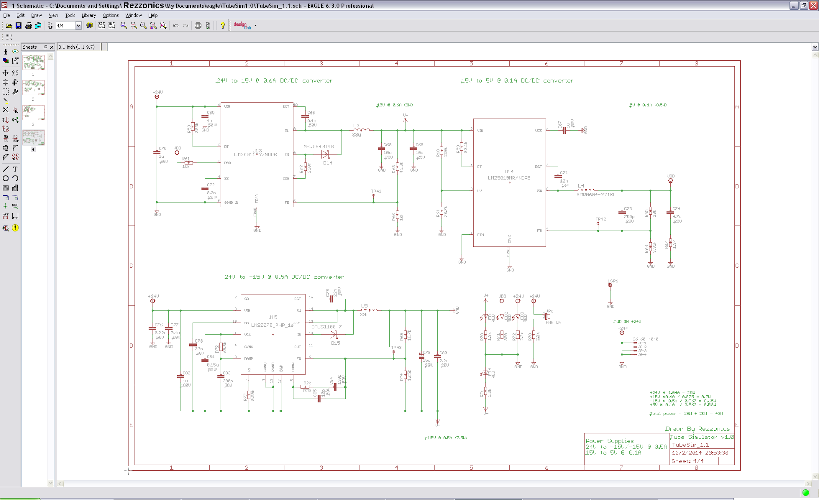
Power Supplies (page 4):
An independent switching power supply module converts 220V AC@50Hz into +24V DC. A Murata MVAD040-24 40W (23 euros) open switching power supply module is used. The module has its own PCB and is mounted inside the box with standoffs and screws.The main PCB is then powered at 24VDC. This is the highest voltage used for output class-D 25W power amplifier.
From 24V, discrete switching regulators generate +15V and +15V to power the operational amplifiers.
From +15V a discrete switching regulator generates +5V to power the headphone amplifier.
The maximun power consumption budget is distributed as follows:
+24V @ 1.1A = 25W for the class D speaker power amplifier (94% efficiency)
+24V to +15V @ 0.6A = 9W for the positive rail of opamps
+15V to +5V @ 0.1A = 0.5W for the headphone amplifier
24V to -15V @ 0.5A = 7.5W for the negative rail of opamps
Total maximum power consumption is 40W
All discrete DC-DC converters have been designed using TI Webench Design Center, a very useful tool for designing power supplies that allows optimizing BoM cost, footprint and efficiency.
The Webench tool generates the whole BoM and it even allows to export schematics and layout to several of the most common CAD applications including Eagle. Sometimes the results are not very good but at least the footprint of mos common components can be created.
Most regulators are based on step-down or buck topology using integrated controllers (power switching MOSFET integrated in the controller device) except for the +24V to -15V that uses inverting buck-boost topology.
The +24 to +15V DC-DC converter is based on TI LM25011 step-down regulator.
The +24V to -15V DC-DC converter is based on TI LM25575 step-down regulator in inverting buck topology
The +15V to +5V DC-DC converter is based on TI LM25019 step-down regulator
This schematic page also includes external Power-on LED and internal SMD power-on LEDs for every power rail: +24V, +15V, -15V and +5V as well as 24VDC power in connector to main PCB from external AC-DC power supply
Subscribe to:
Posts (Atom)