Google statistics

Showing posts with label Texas Instruments. Show all posts

Sunday, 15 May 2016

DMFX-1-1 (main board) schematics and BoM

DMFX-1-1 includes the following blocks:
  • TI C5535 DSP-1 implements the digital effects and audio codec control (pages 2-3)
  • TI AIC3204 ADC/ADC audio codec and buffer, 12MHz clock oscillator, stereo headphones output jack (page 4)
  • DSP-1/2 external memories: SPI, I2C, SD/MMC (page 5)
  • DC/DC step-down switching regulators (3.3V, 1.8V) and LDO (1.3V), power-on reset, clock driver (page 6)
  • FTDI2232 USB/JTAG interface an SEEPROM (page 7)
  • TI C5535 DSP-2 implements LCD, navigator buttons, tuner control (page 8)
  • DMFX-1-2 mezzanine Connectors and footswitch push-button (page 9-10)
  • Line-In stereo input buffer, filters, distortion circuit (page 11)
  • Line-Out dual-mono output buffers and filters, tuner, noise supressor circuits (page 12)
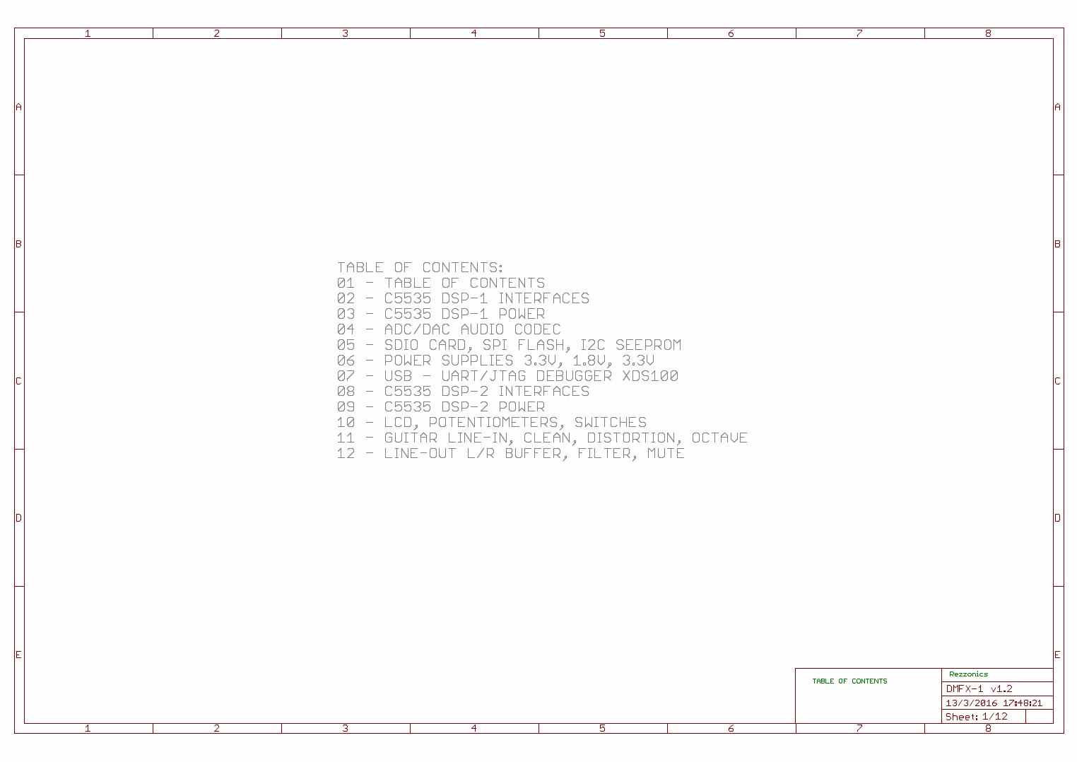
DMFX-1-1: Schematics page 1 - Table of Contents
    DSP-1 implements the digital effects and control the audio codec. It includes a dedicated mini-USB connector. Four analog SAR ADC input are connected to DMFX-1-2 potentiometers. DSP-1 is the first device on the JTAG daisy chain connected to USB/JTAG device to allow JTAG emulation and debugging. INT0 input is connected to DSP-2 external flag (XF) signal and DSP-1 XF signal is connected to DSP-2 INT0; both DSPs exhange interrupts to allow synchronizing processes and tasks between both processors. INT1 is connected to DSP-1 GPIO10. Two SD/MMC cards are connected to DSP-1 to store data, samples, loops, code...
    I2S2 interface is a fast serial interface to exchange samples between DSP-1 and ADC/DAC on audio codec. SPI interface is connected to an external SPI flash to store code and data. UART interface is connected to CBUS on USB/JTAG-UART device and it can be used as console for emulator debugging. I2C bus is connected to external SEEPROM, to store parameters or inventory information. I2C is used for configuring audio codec, and it is also connected to DSP-2 to exchange FX configuration parameters set by user interface via LCD menu and buttons.
    DMFX-1-1: Schematics page 2 - DSP-1 FX interfaces
    Page 2 shows DSP-1 power supply inputs, ferrite filters and decoupling capacitors.
    DMFX-1-1: Schematics page 3 - DSP-FX power

    Page 3 shows TI TLV320AIC3024 audio codec that includes ADC/DAC, LINE input, MIC input, LINE out and stereo headphones amplifier. I2S is a high speed serial interfaces to echange audio samples with DSP-1 at a sampling frequency configured by DSP-1. Interface is buffered via a CBTLV3245 octal bus switch. 12MHz clock oscillator is included here, it is connected to a clock driver on page 6.
    DMFX-1-1: Schematics page 4 - Audio CODEC ADC/DAC
    Page 5 includes two W25Q64 64-Mbit SPI flashes connected to each DSP SPI interface. Two SD/MMC cards are connected to DSP-1 for large storage (samples, loop, data). One I2C 64Kbit SEEPROM 24C64 can be used to store remote inventory or configuration data.
    DMFX-1-1: Schematics page 5 - Memories I2C, SPI, MMC
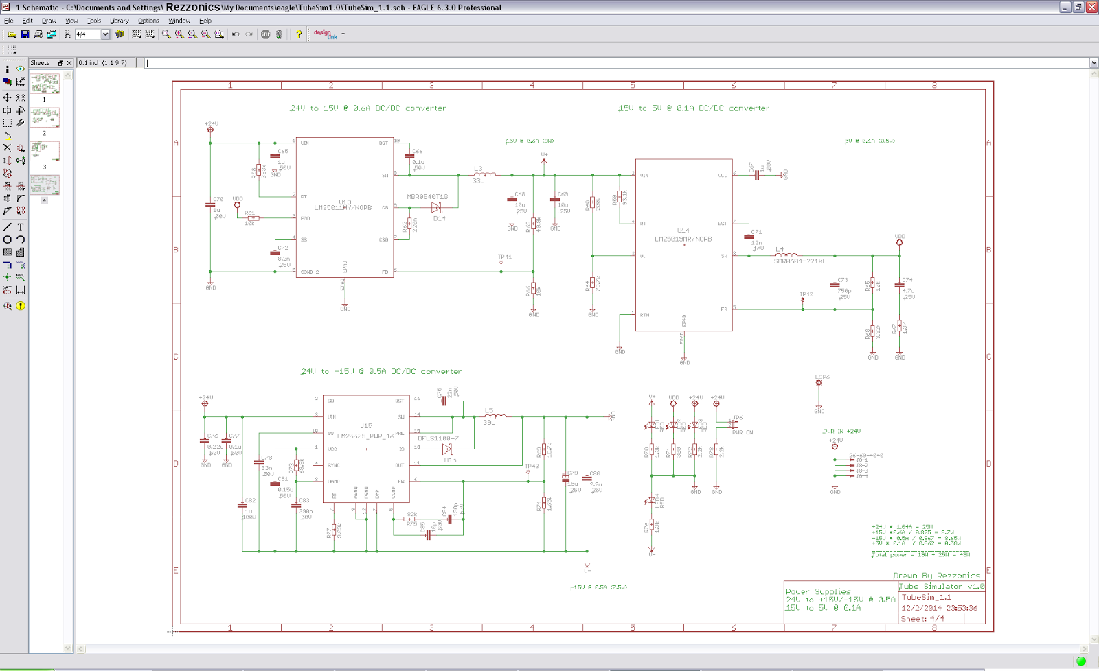
    Page 6 shows two DC/DC step-down switching regulators TI TPS56220. They generate +3.3V and +1.8V respectively from a +9V external supply or +5V USB input with a maximum current of 500mA each. A TI TPS73201 LDO generates the analog 1.3V DSP supply voltage from 1.8V input at a maximum current of 250 mA. A TI CDCLVC1108 octal clock buffer generates up to 8 clocks from 12MHz clock oscillator: USB DSP-1 clock, DSP-1 system clock, audio codec master clock, USB/JTAG clock, USB DSP-2 clock and DSP-2 system clock.
    DMFX-1-1: Schematics page 6 - power supply, clock driver
    Page 7 shows an FTDI2232 USB/JTAG interface device that works as XDS100v2 TI emulator for DSP debugging. ABUS is connected to JTAG daisy chain on DSP-1 and DSP-2. CBUS is sonnected to UART interface on DSP-1. A D-type flip-flop detects power reset rising edge from FTDI device and generates a power detect signal back to the FTDI device. An external SPI SEEPROM AT93C46 stores USB device configuration parameters. USB port is protected for ESD. USB debug port is a type-B USB connector. The +5V USB debug port can be used to power the whole DMFX-1 system. DMFX-1 system can actually be powered from any of the three USB ports or by an external +9V power supply.
    DMFX-1-1: Schematics page 7 - USB/JTAG
    DSP-2 implements user interface and control tasks. It includes a dedicated mini-USB connector. Two analog SAR ADC inputs (AIN0-1) are connected to tuner circuit output and noise supression circuit output respectively, AIN2-3 are connected to DMFX-1-2 potentiometers 2-3. DSP-2 is the second device on the JTAG daisy chain connected to USB/JTAG device to allow JTAG emulation and debugging. INT0 input is connected to DSP-1 external flag (XF) signal and DSP-2 XF signal is connected to DSP-1 INT0; both DSPs exchange interrupts to allow synchronizing processes and tasks between both processors. INT1 is connected to DSP-2 GPIO10.
    DSP-2 GPIO0 controls clean or distorion audio input to audio codec. GPIO1-2 configure the overdrive/distortion gain, GPIO3-4 control different overdrive/distortion modes, increasing mid tones or setting fuzz clipping diodes circuit. GPIO6-11 drive five red LEDs on DMFX-1-2 mezzanine board. GPIO11 is connected to CPU active green LED.
    SPI interface is connected to SPI flash (device 0) and to 128x32 graphic LCD (device 1) on DMFX-1-2 mezzanine board, GPIO12 is connected to LCD A0 signal and is used to send command or data to LCD via SPI bus. GPIO13-17 are connected to the five navigator buttons respectively: left, up, center, down, right.
    GPIO28 is connected to footswitch.
    SPI and UART interfaces are not used. I2C bus is connected to DSP-1 to exchange FX configuration parameters set by user interface via LCD menu and buttons.
    DMFX-1-1: Schematics page 8 - DSP-2 Control interfaces
    Page 9 shows DSP-2 power supply inputs, ferrite filters and decoupling capacitors.
    DMFX-1-1: Schematics page 9 - DSP-2 Control Power
    Page 10 shows DMFX-1-2 mezzanine connectors. J5 connector includes DSP-2 SPI2 bus, LCD A0 addess signal, reset signal and the five navigator button inputs: left, up, center, down, right. J7 connector includes LED1-5, DSP-1 GPAIN0-3 SAR ADC signals, DSP-2 GPAIN2-3 SAR ADC signals, distortion circuit output, octave circuit output and the mix of distortion-octave coming from a potentiometer on DMFX-1-2. +3.3V, analog +1.3V power supplies and ground.
    DMFX-1-1: Schematics page 10 - Connectors
    Input buffers and filters and distortion circuits are based on TI rail-to-rail LME49721 audio op-amps powered at +3.3V, in contrast with +9V supply normally used on guitar pedals. 

    Overdrive/Distortion:

    First opamp stage has 0dB gain but implements some low pass filtering. Second op-amp stage implements a configurable gain controlled by DSP-2 GPIO signals connected to OD_DRV0-1. when both switches are active (shorted) we obtain the minium gain value of 13dB (x4.5), if OD-DRV1 is open, gain value is incremented by 10dB (x14.5), if OD_DRV0 is open, gain value is incremented by 9dB (x40). Third op-amp stage implements high saturating gain (hard clipping) or soft clipping via asymmetric diodes, when OD_MODE1 is 0, a 20dB gain is implemented with 10K switch shorted and switch in series with diodes open. When OD_MODE0 is 1, a 10dB gain is implemented, but soft asymmetric clipping is added with Schottky diodes added in parallel to the opamp feedback path.

    OD_MOD0 activates a notch filter that attenuates middle tones by 12dB at 400Hz.

    These four GPIOs: OD_DRV0-1 and OD_MODE0-1 allow different combinations of gain, hard clipping, soft clipping, and mids attenuation to get different types of analog overdrive and distortion effects.

    Octave-up:

    A forth op-amp implements a full-wave rectification that generates a octave up, that can be mixed with distortion output.

    Line-In circuit:

    The input from a guitar can be connected to Line-In input. The first stage is a J-FET buffer, followed by a filter that boosts up to 6dB high frequencies and attenuates down to 9dB low frequencies. 0dB occurs at 3.7kHz. The filtered line-in signal is the input to the tuner circuit and to an analog switch that can select the clean or the distortion at its output. The output of the switch is connected to the Audio Codec analog left channel input. Right channel input is connected to the clean signal, this allows mixing clean and distorted signal within DSP and obtain a more or less overdriven signal.
    The op-amp at the bottom of the page is a follower buffer that generates a middle point reference signal at 1.65V equal to 3.3V/2. Op-amps are rail-to-rail TI LME49721 powered at 3.3V.
    DMFX-1-1: Schematics page 11 - Input buffers, filters, clean, distortion
    Page 12 shows right and left channel pre-amp circuit with high impedance Line-Out signals that can be connected to a guitar amplifier or Line-In input of a sound card or sound equipment.This pre-amp amplifies 9dB with a 3dB bandwidth of 1.35kHz, 0dB is at 4kHz. The first op-amp stage filter is a low pass filter with a pole at approximately 14kHz and 3dB bandwisth at 24 kHz.

    The two op-amp circuit at the bottom of the page is used as support to the tuning and noise suppression circuit within the control DSP-2. The first stage is a very high gain amplifier that can be used as power detector for a noise suppression algorithm. The second op-amp is used as comparator and generates a square wave between 0 and full scale with the same fundamental frequency as the input signal and zero voltage when no signal is present. This square wave simplifies tuning algorithm using and auto-correlation method. Both tuner and noise suppression signals are connected to analog inputs of SAR ADC circuits within the Control DSP-2
    DMFX-1-1: Schematics page 12 - Output buffers, filters, tuner, noise suppression

    Schematics and BoM source files

    Schematics and layout have been made using CAD Eagle 6.3.0. Source files can be found in the DMFX-1-1 github HW repository including Eagle Schematics source files (.sch), Eagle Board layout files (.brd), Eagle component libraries (.lbr), Schematics in pdf format, and all manufacturing files including gerber files, assembly drawings and pick and place files. An Excel file contains the full BoM including reference designators, manufacturer part number  as well as Digikey part number.

    For your convenience here is a link to DigiKey with a BoM of the whole DMFX-1 platform including main board DMFX-1-1, described in this post, and the daughter board (DMFX-1-2 with LCD and navigator buttons). You'd better verify BoM completion, lead-times and obsolescent components beforehand.

    With all this information you can build your own DMFX-1 platform and develop your own Digital effects!!

    Friday, 18 July 2014

    Tube Simulator - Practical implementation - Schematics, BoM (1/4)

    For the practical implementation of the Tube Simulator, Eagle CAD was used for schematics capture and PCB layout.

    Component Selection and Bill of Materials:

    SMD devices where used for smaller sizer, 0603 resistors are a good compromise between easy hand solderability and small size.

    Texas Instruments LME49723 audio dual operational amplifier was chosen as a good compromise between low distortion, quality, cost, size, nice SOIC packaging and high power supply voltage.
    I particularly like TI website for its quick and easy selection of components by means of a parameters table and a large choice of components.

    Even though I am a big fan of MLCC (multilayer ceramic capacitors) I read in a series of articles in EDN website (Signal distortion from high-K ceramic capacitors and the follow-up More about understanding the distortion mechanism of high-K MLCCs) that film capacitors are better suited for audio applications since they are more linear in its frequency response and have less harmonic distortion than ceramic capacitors. MLCC capacitors experience large changes in capacitance as the voltage across them changes, which can result in harmonic distortion. So I decided to use film capacitors everywhere where the capacitor value was key to filtering the audio signal.

    But I still used MLCC for signal bypassing and power supply decoupling.

    The BoM was created in the Mouser website, with a huge selection of components and hardware

    This is the link to he whole Bill of Materials on the Mouser website:

    Input Preamp and Output Amp Schematics (page 1)


    Each opamp stage is based in the aforementioned LME49723 device consisting of two opamps.

    In the first opamp stage, zener diodes are used to clip signal levels. A 6.2V zener diode BZX84C6V2LT1G is used in the positive cycles and a 4.3V zener diode BZX84C4V3LT1G is used in the negative cycles.

    After the first opamp stage a Schottky diode BAT54 in series with a 470k resistor is used for soft clipping, this provides a clipping closer to germanium diodes.

    On the second opamp stage there is a feedback branch with a NPN transistor (MMBT2907ALT1SMD) which has its base biased at 1.65V, a TI LM4041CIDBZ shunt voltage reference was used. Another feedback branch uses a 2.7V zener diode BZX84C2V7LT1G in series with a diode MMBD4148 and a 470ohm resistor for clipping negative cycles. A third branch used another 2.7V in series with a higher 10K resistor for soft clipping of positive cycles.

    The third opamp stage is just a follower to send the signal to an external effect circuit and to the output amp section. The return is also input to this stage.

    An equivalent circuit to the VOX AC30 bass/treble equalizer is placed at the input of the output amp section. The equalization switch adds a deeper mid notch when activated.

    The first opamp stage of the output amp adds harder clipping with two silicon diodes MMBD4148 in parallel for clipping both positive and negative cycles. And also a schottky diode in series with a 47 ohm resistor that provides a kind of germanum diode clipping in the negative cycles.

    The second opamp stage adds additional clipping in both cycles by using silicon diodes MMBD4148.

    A log 100K potentiometer provides volume level control of the output amp.
    The forth opamp is a double follower that sends the signal to the speaker simulator and the Line out connector.

    Speaker Emulator and Headphone Amplifier Schematics (page 2)

    The second page of schematics shows the speaker emulator circuit based on four Sallen-Key low-pass filter sections to provide a frequency response similar to that of a 12'' speaker like Celestion Vintage 30, as shown in a previous post. This filter enhances considerably frequencies around 2.5 kHz.

    A log 100K potentiometer provides speaker emulator volume level.

    A switch selects Line out signal from the speaker emulator output or the output amp to be connected to an external guitar amplifier.

    The headphone input is always selected from the speaker emulator output.

    The headphone amplifier used is a TI TPA6111A2D 150 mW stereo headphone amplifier in a SOIC-8 device connected to a 3.5 mm mini-jack.

    25W Class D Amplifier, mounting holes, fiducials (page 3)

    The third page of the schematics shows the 8ohm speaker amplifier based on a very efficient (94%) 25W Class-D amplifier TI TPA3112D1PWP with less than 0.1% THD+N from a +24V supply.

    The high efficiency of this new class-D amplifiers allows a relatively high power output of 25W without the need of a heatsink on a small HTSSOP 28-pin device which considerably reduces PCB layout size. Special careful must be taken with the design of the central pad connected to the ground plane by numerous vias to allow proper heat dissipation.

    Power Supplies (page 4):

    An independent switching power supply module converts 220V AC@50Hz into +24V DC. A Murata MVAD040-24 40W (23 euros) open switching power supply module is used. The module has its own PCB and is mounted inside the box with standoffs and screws.

    The main PCB is then powered at 24VDC. This is the highest voltage used for output class-D 25W power amplifier.
    From 24V, discrete switching regulators generate +15V and +15V  to power the operational amplifiers.
    From +15V a discrete switching regulator generates +5V to power the headphone amplifier.

    The maximun power consumption budget is distributed as follows:
    +24V @ 1.1A = 25W for the class D speaker power amplifier (94% efficiency)
    +24V to +15V @ 0.6A = 9W for the positive rail of opamps
    +15V to +5V @ 0.1A  = 0.5W for the headphone amplifier
    24V to -15V @ 0.5A = 7.5W for the negative rail of opamps

    Total maximum power consumption is 40W

    All discrete DC-DC converters have been designed using TI Webench Design Center, a very useful tool for designing power supplies that allows optimizing BoM cost, footprint and efficiency.

    The Webench tool generates the whole BoM and it even allows to export schematics and layout to several of the most common CAD applications including Eagle. Sometimes the results are not very good but at least the footprint of mos common components can be created.

    Most regulators are based on step-down or buck topology using integrated controllers (power switching MOSFET integrated in the controller device) except for the +24V to -15V that uses inverting buck-boost topology.

    The +24 to +15V DC-DC converter is based on TI LM25011 step-down regulator.
    The +24V to -15V DC-DC converter is based on TI LM25575 step-down regulator in inverting buck topology
    The +15V to +5V DC-DC converter is based on TI LM25019 step-down regulator

    This schematic page also includes external Power-on LED and internal SMD power-on LEDs for every power rail: +24V, +15V, -15V and +5V as well as 24VDC power in connector to main PCB from external AC-DC power supply