I purchased some KORG NuTube 6P1 triodes samples and I wanted to build a guitar preamp circuit to get the characteristic tube sound and distortion.
I could not find any guitar preamp amplifier schematics that would suit me so I decided to make my own circuit based on the reference circuit and add some gain, tone stack and volume controls
I am more of a "SPICE simulation" kind of guy than a "bread-boarding" guy, also because I like to use SMD components and try to be closer to the final guitar pedal than just a prototype. I have quite some confidence in SPICE results provided that models are accurate.
I wanted to simulate my NuTube circuit before building a guitar pedal or amp. The problem is that there were no NuTube SPICE models available.
I found that Koren had obtained a method for obtaining tube SPICE parameters from datasheet curves plate current (Ip) vs plate-cathode voltage (Vpk) for variable Vgk (grid-cathode voltage). Actually the models I have from traditional triodes, all come from using this method.
I downloaded Koren's
MATLAB program and followed his instructions for
Finding SPICE tube model parameters.
The task showed to be more difficult than I thought, convergence of the method did not work very well, and I had a lot of tuning to make.
These are the current-voltage curves from the datasheet:
The following figure shows the curves I obtained in MATLAB using Koren's approximation method with the points taken from NuTube datasheet:
There is some dispersion in the curves from the datasheet points but that was the best I could get.
This is the NuTube 6P1 SPICE model I got:
.SUBCKT NU6P1_l 1 2 3 ; P G C (Triode)
X1 1 2 3 TRIODE MU= 18.10 EX= 4.080 KG1=4270851.9 KP=451.94 KVB= 4.2 VCT= 0.00 RGI=330k CCG=9.1P CGP=2.5P CCP=4.3P
* http://www.nutube.us/downloads/Nutube_Datasheet_31.pdf 13-May-2017
.ENDS
And this is Koren's 12AX7 model:
.SUBCKT 12AX7 1 2 3 ; A G C (Triode) OLD MODEL AKA ECC83
* Original Koren Model
X1 1 2 3 TRIODE MU=100 EX=1.4 KG1=1060 KP=600 KVB=300 VCT=0.00 RGI=2000 CCG=2.3P CGP=2.4P CCP=.9P ; ADD .7PF TO ADJACENT PINS; .5 TO OTHERS.
.ENDS 12AX7
Mu is 18, much lower than 12AX7 with a value around 100.
The exponent EX is quite high, around 4, compared to 1.4 on the 12AX7
A high KG1 value corresponds to a low plate current.
KP which is used in the high plate voltage region is 452 compared to 600.
KVB knee voltage is 4.2, much lower than 12AX7 value of 300.
RGI, CCG, CGP and CCP are obtained from the Datasheet.
Anyway, I had my NuTube 6P1 SPICE model and I could start designing and simulating my guitar preamp.
Then the user
Teemuk from
DIYstompboxes forum posted
an interesting comment on this thread, where he believed that
KORG NuTube 6P1 response was not much different from a traditional tube (like
12AX7 or 12AZ7) in "starved" mode, that is, with a low plate/anode voltage.
There are several advantages praised by KORG about this NuTube: smaller size, higher reliability and low power voltage.
But if a similar response is obtained from a traditional "starved" tube powered at the same low voltages, one of the most important advantages does not exist anymore.
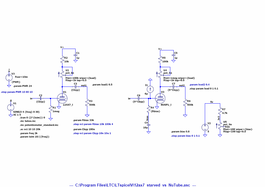
So I decided to try to make a comparison between them using LTSpice.
Unfortunately, according to some reports, it appears that existing SPICE models do not work well in the starved region, these are approximated models, and the starved region is just a tiny area in the curves that go up to 400V.
But I knew how to get SPICE parameters models from curves, so if I could find accurate current/voltage curves in the starved region I could make a model suited for those low voltages.
I then found this study on the net:
Triodes at Low VoltagesLinear amplifiers under starved conditions.By Merlin Blencowe
that showed these curves on the starved region obtained experimentally:
Again, using the Koren's method I got the following current-voltage approximated curves for 12AX7 triode:
And again, there is some dispersion in the curves from the experimental points. The worst dispersion happens at the knee at Va=1V for Vgk=0V, where plate current is around 60uA instead of 100uA.
This is the obtained 12AX7 starved model:
.SUBCKT 12AX7_l 1 2 3 ; P G C (Triode)
X1 1 2 3 TRIODE MU= 81.48 EX=0.626 KG1=1865.5 KP=248.15 KVB=300.0 VCT=0.00 RGI=2000 CCG=2.3p CGP=2.4p CCP=0.9p ;
* http://www.valvewizard.co.uk/Triodes_at_low_voltages_Blencowe.pdf 24-May-2017
.ENDS
Mu is lower, Exponent EX is lower, KG1 is higher (lower plate current), KP is lower and KVB is the same.
These same curves can now be simulated using LTSpice. These are the schematics:
Starved 12AX7 plate current is then drawn with plate-cathode Vpk voltage (V2) varying from 0V to 24V in 0.1V steps, using grid-cathode voltage Vgk (V1) as a parameter varying from -0.5V to 0V in 0.1V steps:
The following figures show NuTube 6P1 current-voltage curves obtained from LTSpice with plate-cathode Vpk voltage (V2) varying from 0V to 30V in 0.1V steps, using grid-cathode voltage Vgk (V1) as a parameter varying from 0V to 4V in 0.5V steps compared to scaled values from datasheet: